Wiki DLP4100 » History » Revision 27
« Previous |
Revision 27/60
(diff)
| Next »
Frédéric Blanc, 2017-04-26 08:58
Wiki DLP4100
Overview

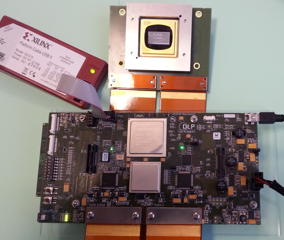
The DLP® Discovery™ 4100 (D4100) is the latest in a series of spatial light modulation development kits from Texas
Instruments. Users of the D4100 Starter Kit have the ability to manipulate visible, ultraviolet and near-infrared light
with extremely high performance and high resolution.
The D4100 offers developers a flexible platform to design products to fit most any application using the proven
reliability of DLP technology.

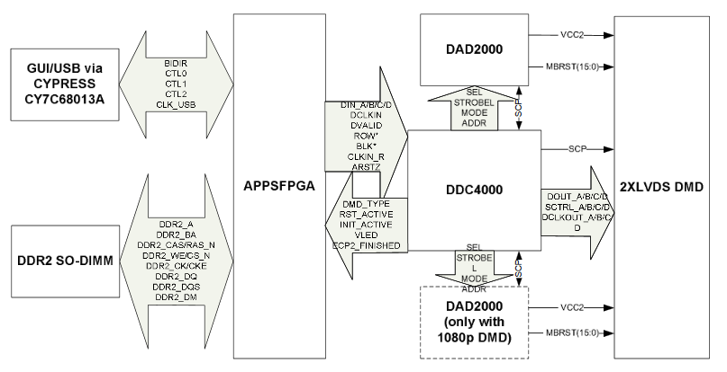
Fig 1: System Overview
| New version | Actual | Name |
|---|---|---|
| DLPC410 | DDC4100 (FPGA X5VLX30) | Digital Controller for Discovery 4100 chipset |
| DLPR410 | XCF16 | PROM for Discovery 4100 chipset |
| DLPA200 | DAD2000 | DMD Micromirror Driver |
DLPC410 DLP Digital Controller [dlps024c.pdf]
Configuration Jumpers, Switch and LED

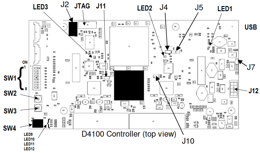
Fig 2: D4100 Controller Configuration Jumpers, Switch and LED
CY7C68013A_128
LED2 - APPSFPGA status
(FPGA PIN N14)
| LED | Status |
|---|---|
| RED | BAD |
| GREEN | OK |
LED3 - DDC4000 status
| LED | Status |
|---|---|
| RED | BAD |
| GREEN | OK |
LED9..12 - LED status
LED9 - DDC_LED0 Status LED for the DDC4000
The LED0 signal is typically connected
to an LED to show that the DLPC410
is operating normally.
The signal is 1 Hz with 50% duty cycle,
otherwise known as the heartbeat
LED10 - DDC_LED1 Status LED for the DDC4000
The LED1 signal is typically connected to an LED
indicator to show the status of system initialization
and the status of the clock circuits. The LED1 signal
is asserted only when system initialization is
complete and clock circuits are initialized. Logically,
these signals are ANDed together to show an indication
of the health of the system. If the Phase Locked
Loop (PLL) connected to the data clock and the DMD
clock are functioning correctly after system
initialization, the LED will be illuminated
LED11 - VLED0 This logic is to be defined by the APPSFPGA application. Drive low to turn on the led. Drive high to
turn off the led(FPGA PIN AK19).
LED12 - VLED1 This logic is to be defined by the APPSFPGA application. Drive low to turn on the led. Drive high to
turn off the led(FPGA PIN AJ19).
J2 – EXP Voltage Select
J4 – Used to select the revision of firmware loaded from the PROM to the APPSFPGA.
| Jumper Position | Revision Version |
|---|---|
| open | 0 |
| close | 1 |
J5 – Shared USB signal disabled
| Jumper Position | USB Signals |
|---|---|
| 0-1 | Disconnected from FPGA |
| 1-2 | Connected to FPGA |
| 2-3 | Automatically connect USB signals to FPGA when USB is connected to host PC |
J7 – USB EEPROM Programming Header
Used to temporally disconnect the USB EEPROM fromthe device so the device can load its internal
boot loader rather than any code in the EEPROM. Install J8 for Cypress internal boot loader.
J10 – DAD2000 B Output Enable
Used to enable the outputs for DAD2000 B. This needs to be enabled only if using the 1080p DMD,
otherwise this can be disabled.
| Jumper Position | DAD2000 B Outputs |
|---|---|
| open | Disabled |
| close | Enabled |
J11 – Used to select the revision of firmware loaded from the PROM to the DDC4100 (FPGA X5VLX30).
| Jumper Position | Revision Version |
|---|---|
| open | 0 |
| close | 1 |
SW1 - Dipswitches
Functionality defined by APPSFPGA programming. In default test pattern code:| Switch Number | Effect | FPGA PIN |
|---|---|---|
| 1 | ON = float – float all mirrors | G20 |
| 2 | ON = counter halt – stop counter, this will freeze the image on the DMD | G21 |
| 3 | ON = complement data – causes DDC 4000 to complement all data it receives | F20 |
| 4 | ON = north/south flip – causes the DDC 4000 to reverse order of row loading, effectively flipping the image |
G22 |
| 5 | Dictates the type of reset being used LSB ON = 1 | H15 |
| 6 | Dictates the type of reset being used MSB ON = 1 | H14 |
| 00 : single block phased reset | ||
| 01 : dual block phased reset | ||
| 10 : global reset | ||
| 11 : quad block phased reset | ||
| 7 | ON = Row Address Mode | H12 |
| 8 | ON = WDT Enable, disables other resets | J14 |
SW2 - Push Button Momentary Switch
Functionality defined by APPSFPGA. This switch is used for APPS_LOGIC_RESET in the default code.
(FPGA PIN T24)
SW3 - Push Button Momentary Switch
Functionality defined by APPSFPGA. This switch is used for APPS_LOGIC_MIRROR_FLOAT in the default code.
(FPGA PIN P10)
SW4 - POWER STANDBY
USB
The USB EEPROM does not have any code only VID/PID data. Here is a sequence of USB initialization:
When a board is plugged in by USB the Windows D4100 USB driver sees the unprogrammed TI VID/PID.  (The Windows D4100 USB driver is installed with the Explorer software.)
    Then it loads a program directly into the Cypress USB (not the EEPROM) and runs it.  (This loads the firmware through USB)
    This sets the Cypress VID/PID to show that the part is programmed and allows communication with the Board.
This is only the first part. To communicate with the DMD a different APPS_FPGA program (D4100_GUI_FPGA.bin) must be loaded that can communicate with the Cypress USB.
When the D4100 Explorer is started it checks to see if D4100_GUI_FPGA.bin is loaded in the FPGA and programs the FPGA if it not.
This program can also be loaded by invoking the DLL function directly from another program (see the API Programmer’s Guide)
Once loaded then the other API DLL functions can be used to load and reset image data.
If you have one of the ViALUX ALP versions you will need to contact them concerning this since their software uses proprietary communication protocols with the D4100.
Updated by Frédéric Blanc over 7 years ago · 60 revisions